


Products & Technology

-
Example of FMM Caught by Jig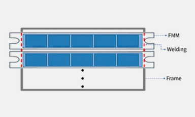
-
FMM Used for OLED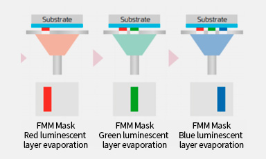
-
Graphene MSAP_FMM
Currently, the FFM market has problems such as W company's base substrate separation and plating quality problems, A company's Burr removal limit and Sharp adjustment problems, and D company’s over-etching and non-etching problems.
In contrast, GrapheneLab Co., Ltd. ensures high yield through a method of conductive material (CVD graphene) based on graphene.
Currently, it occupies the exclusive market of D Company in Japan, and export sanctions are being developed during the exclusive supply to S Company.
Two companies are under development in Korea, but they have no performance so far and are negative for the following reasons.
| Method | Issue | Possible Future | Strength / Developer |
|---|---|---|---|
| Based Graphene | Issue Expensive CVD graphene manufacturing equipment |
Possible Future Price lowered by mass orders |
Strength / Developer Method by conductive material(CVD Graphene) / GrapheneLab |
| Electro-forming |
Issue Issue about based board separationIssue about plating quality |
Possible Future Mass production limited by quality issue |
Strength / Developer W Company |
| Laser |
Issue Limitation in Burr separation Issue about adjustment of hall structure (sharp) |
Possible Future Market entrance is unclear due to fine pattern limitation for hall |
Strength / Developer A Company |
| Etching |
Issue Over-etching, under-etching |
Possible Future Market entrance is expected to be difficult due to the barriers of S & D companies |
Strength / Developer D Company |
-
01
Purpose
Electroforming with electrodes allows fine forming
Used as a base substrate when manufacturing a metal screen with a fine pattern
Improvement of a defect in electroplating peeling of fine PPI
-
02
Feature & Merit
Easy to form fine patterns
Electroplating Process Optimization Specifications
Easy to peel off metal screens with fine patterns below 30
Process yield can be 90% or higher when using electroplating substrates
Metal Screen During
the electroplating process Process yield Possible
More Than
90%

CEO : Kwon Yong Duck
Charge Of Privacy Policy : Kim Hyun Woo
Company Registration Number : 280-86-01050
Office Location : 9-13, Dongtansandan 4-gil, Hwaseong-si, Gyeonggi-do
Tel : +82-31-378-2559 Fax : +82-31-377-2538